
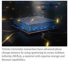
Tohoku University researchers have made significant advancements in phase change memory technology by utilizing a sputtering process to create niobium telluride (NbTe4), a material known for its exceptional storage and thermal capabilities.
Phase change memory is a type of nonvolatile memory that harnesses the unique properties of phase change materials (PCMs). These materials can transition between an amorphous state, where atoms are randomly arranged, and a crystalline state, where atoms are highly ordered. This reversible phase change produces distinct electrical properties that can be precisely engineered to store and retrieve data.
While phase change memory is still a relatively young field, it holds the potential to revolutionize data storage due to its high storage density and faster read and write speeds. However, the intricate switching mechanisms and complex fabrication processes associated with these materials have posed challenges for mass production.
In recent years, researchers have turned their attention to two-dimensional (2D) Van Der Waals (vdW) transition metal di-chalcogenides as promising candidates for PCM applications in phase change memory. Now, a team of scientists from Tohoku University has showcased the potential of sputtering as a fabrication technique for large-area 2D vdW tetra-chalcogenides. Using this method, they successfully created and identified an exceptionally promising material—niobium telluride (NbTe4)—with an ultra-low melting point of approximately 447 ºC (onset temperature), setting it apart from other transition metal di-chalcogenides (TMDs).
“Sputtering is a widely adopted technique that involves depositing thin films of a material onto a substrate, offering precise control over film thickness and composition,” explains Yi Shuang, an assistant professor at Tohoku University’s Advanced Institute for Materials Research and co-author of the research paper. “Our deposited NbTe4 films initially exhibited an amorphous structure but could be crystallized into a 2D layered crystalline phase by annealing at temperatures above 272 ºC.”
This breakthrough in utilizing sputtering to create large-area 2D vdW tetra-chalcogenides, particularly NbTe4, opens up new possibilities for phase change memory technology. NbTe4’s remarkable thermal properties and low melting point make it a standout candidate for improving the efficiency and scalability of phase change memory devices. As researchers continue to refine the fabrication processes and harness the unique properties of materials like NbTe4, the potential for phase change memory to reshape data storage technologies becomes increasingly promising


Customer Reviews
Thanks for submitting your comment!